
Semiconductor Yields and Binning: When good chips go bad

As transistors get smaller, manufacturers are able to place more of them into the same amount of area. Apple’s M2 Ultra consists of 134 billion transistors1, Nvidia’s Hopper-architecture GPUs boast 80 billion transistors2, and Cerebra’s “wafer scale” CPU has an incredible 1.2 trillion transistors34. What happens if even one of these transistors is bad? With so many of these devices crammed onto a die, how do manufacturers make sure that every single one works right?
The answer: They don’t.
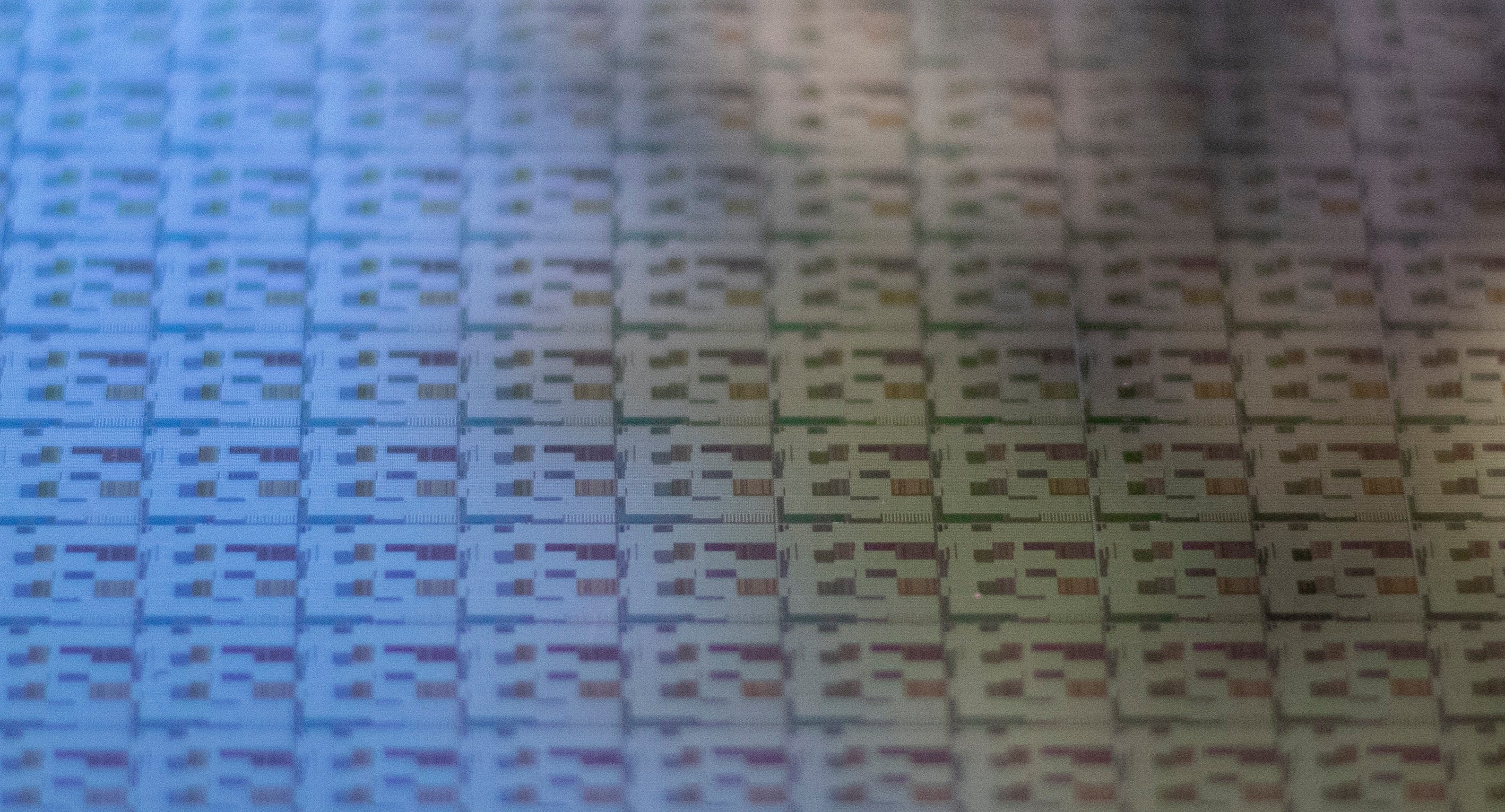
Manufacturing integrated circuits is really, really difficult. It involves a process called photolithography where light is used to etch patterns onto a silicon wafer, and it must be done very, very precisely. When making a die using the 3 nm process5 if the wafer were to move or shake the distance of even just a few atoms while etching, the entire device could be ruined. The doped silicon must be extremely pure and handled in an environment free of contamination: the air within the clean rooms at foundries is orders of magnitude cleaner than that within hospital operating rooms. The physical act of chopping up the wafer and putting it into it’s plastic or ceramic packaging can damage the chip, so can the act of soldering it onto a PCB.
The point being that for devices with hundreds of billions of transistors on them, it’s inevitable that a few of them are going to be bad. Sometimes the chips are just total duds: they have such serious defects that they won’t power on, they won’t boot up, or they are just otherwise unusable. In the industry the ratio of total chips you tried to manufacture versus the total number of chips that actually work is known as your “yield”, and manufacturers obsess over their yields.
Yields are what make or break semiconductor companies. It’s not just about knowing how to make chips, it’s about knowing how to make them consistently enough to be profitable. For example, “Multiple patterning” is a process that can be used to make cutting-edge tiny transistors with simpler, cheaper machinery (that is, without the use of something like an extreme ultraviolet (EUV) lithography machine), which involves performing multiple etchings or “exposures”. But multiple patterning is prone to low yields6: if some of the exposures are just slightly misaligned, multiple dies can be ruined. So while it works, it produces such bad yields that it’s simply not economical for the latest process nodes.
So what can you do to improve yields?
The first and most obvious step is to improve the manufacturing process. Make the air cleaner, find ways to make the machines shake less, use better, more accurate lithography machines, tweak the size and shape of the transistors, find better ways of cutting the wafers, etc.. Every manufacturer has their own secret sauce of these little tweaks called the “best known method” or BKM, and they are fiercely guarded trade secrets78.
Another action the designers of the chip take is to add redundancy to their chips. Circuits are occasionally designed in such a way that even if a few transistors within it fail, the circuit overall will still be able to function. But redundancy is costly, complex, and only effective up to a certain point.

But there’s one technique manufacturers use to improve yields above all else: binning. Sometimes defects occur in very critical parts of the chip, and it’s rendered unusable. But if the defect is in a non-critical part of the chip, you can just choose not to use that part. Suppose you’re making a processor with 4 cores, and one of the cores has a serious defect in it. Why throw the whole thing away, when you could sell it as a 3 core chip instead? What if you have a 4 mb cache but only 2 mb of it works? Well you can sell it as a device with a smaller cache. This called “binning” because as different parts of the chip fail you can put them into different categories or “bins”: here’s some processors where not all the cores work, here’s some processors with busted GPUs, here’s some processors that are missing video encoders/decoders, here’s some processors with both some busted cores and a busted GPU, etc..
Binning goes further than just “failed” parts. Sometimes the transistors on one device behave better than transistors on another device. This can mean that they use less power (that is, the transistors are less leaky), or the transistors have faster switching speeds. If you take two integrated circuits of the same design but from two different wafers and compare them, they will likely draw different amounts of power and have different max clock speeds even if they have no functional defects.
You’ve probably encountered binning before and not known it if you’ve ever built your own PC. When buying a processor, you may notice that Intel and AMD offer a confusingly large selection of processors with different cores, cache sizes, GPU capabilities, max frequencies, power consumptions, etc., and it’s all because of binning. AMD and Intel know that their long list of SKUs is confusing and overwhelming to customers, but that’s a far preferable alternative to tossing perfectly good hardware.
If you buy an Intel i7, you’re probably actually buying an Intel i9 with some busted internals. And if you noticed while shopping that some processors have higher clock speeds than others despite being the latest tech and having the same specs, that’s binning too. One of the chips just happened to have some leaky or slow transistors. Intel, AMD, and all the other chip designers and manufacturers are not wasting their resources making this huge variety of lower-end chips. They’re only making their best, but through binning they’re able to allow for failures to happen in the manufacturing process and still produce usable hardware.
Lastly I’ll mention a relatively new way of improving yields: chiplets! Instead of manufacturing a device on one big rectangle of silicon, what if you made all it’s components individually (like it’s GPU, processor cores, hardware accelerators, etc.) on their own smaller silicon die, and then wired them together afterword? That way, if you’re interested in making only “perfect” chips, instead of throwing away the entire device when a component has gone bad, you only need to replace that one component. Chiplets are often also designed to be modular, so that engineers can mix-and-match them like Lego pieces and create new chips without having to design a whole new silicon floorplan from scratch.
Semiconductor manufacturing is a very, very complex field that makes very, very complex products where defects are unavoidable. With binning, companies have a way to drastically reduce waste and improve yields which not only makes business sense, but is also better for the environment and gives consumers more variety at different price points. Sometimes it’s not about doing things perfectly, it’s about finding smarter ways to handle the inevitable defects.

Cerebra’s processor was manufactured starting in 2019 using TSMC’s 16nm FinFET process which is relatively old and large as of January 2024, so what it lacks in density it makes up in sheer size: the silicon die alone measures 8 inches by 9 inches!
Manufacturers name their technologies very confusing things, the 3 nm process doesn’t actually mean that the transistors themselves are 3 nm wide/tall, it’s purely a marketing term. Transistors made using this process are actually on the order of around 50 nm in size.
Prone to low yields today. As the industry is moving towards 13.5 nm EUV lithography machines, multiple patterning is being used to eek out the remaining usefulness of the older 193 nm machines with diminishing returns.
So too are the yield numbers for a given BKM a top secret metric. You don’t want your competitors knowing how good (or bad) you’re doing.
Awesome job on this! I get to work on yield / binning and it’s so rewarding.